Electron Microscope
- Products
- Petroleum & Oil Testing
- Flash Point Tester
- Engler Viscometer
- Water Content Tester
- Kinematics Viscometer
- Distillation Tester
- Density Tester
- Rust & Corrosion Tester
- Sulphur Content Tester
- Acid & Alkali Tester
- Dropping Point Tester
- Demulsibility Tester
- Aniline Point Tester
- Ash Content Tester
- Low Temperature Tester
- Residue Carbon Tester
- Existent Gum Tester
- Vapor Pressure Tester
- Oxidation Stability Tester
- Foaming Characteristic Tester
- Bomb Calorimeter
- Octane & Cetane Analyzer
- Other Tester
- Tablet Drug Tester
- Dissolution Tester
- Disintegration Tester
- Tablet Hardness Tester
- Friability Tester
- Multi-Purpose Tester
- Clarity Tester
- Gelatin Gel Strength Test System
- Bloom Viscosity Tester
- Thaw Tester
- Melting Point Tester
- Moisture Tester
- Transparency Tester
- Vacuum Constant Temperature Drying Case
- Transdermal Diffusion Tester
- Gelatin Freezing Strength
- Refrigeration & Cryogenic
- Life Sciences
- Laboratory
- Spectrometer
- Spray Dryer
- Rotary Evaporator
- Reactor
- Sterilizing & Cleaning
- Water Quality Analyzer
- Chemical Analysis
- Physical Testing
- Centrifuge
- Pathology Equipment
- Optical
- Ultrasonic Homogenizer
- Packaging Testers
- Compression Testing Machine
- Water Vapor Permeability Tester / Moisture Permeability Tester
- Air Permeability Analyzer
- Tearing Tester
- Heat Sealer
- Seal Tester
- Oxygen Permeability Tester
- Friction Tester
- Falling Dart Impact Tester
- Horizontal Impact Tester
- Pattern Thickness Tester
- Evaporated Residues Tester
- Inverted Pressure Sterilized Boiler
- Electronic Tensile Tester
- Heat Shrink Tester
- Leakage Tester
- Hot Tack Tester
- Disc Peeling Tester
- Roller Pressing Machine
- Sample Cutter
- Spectrodensitometer
- Hot Sticky Pull Tester
- NDT
- Agriculture & Food
- Hazardous Chemical Detection
- Fusion Machine
- Testing Chamber
- Filter Integrity Tester
- Petroleum & Oil Testing
- Industry Testing Device
- Featured


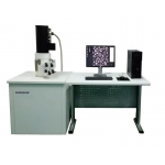
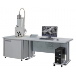
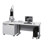
Scanning probe microscope
SPM550
The scanning tunneling microscope is a non-optical microscope that scans an electrical probe over a surface to be imaged to detect a weak electric current flowing between the tip and the surface.
- Remove this product from my favorite's list.
- Add this product to my list of favorites.
More info
Performance Index
- International mainstream research-grade professional equipment, integrated atomic force microscope (AFM), lateral force microscopy (LFM), scanning tunneling microscopy (STM) (SPM550A STM does not have the feature)
- Resolution (60μm scanner):
AFM (Atomic Force Microscope): horizontal 0.2nm, vertical 0.03nm (mica crystals calibration)
STM (Scanning Tunneling Microscopy): transverse 0.1nm, vertical 0.01nm (graphite crystal calibration)
- High-precision measurement standard sample type instrument, using NanoSensors provides traceable to international measurement authority Physikalisch-Technische Bundesanstalt (PTB) for calibration
- One-key speed full automatic injector, without manual presetting, travel > 30mm, which can accommodate large samples, maximum sample size 45mm × 45mm × 30mm (SPM550LS maximum sample sizes up to 102mm × 102mm × 30mm)
- Samples can be read two regulatory agencies which can be accurately positioned detection area
- Optional software control visualization 2D electronically controlled sample mobile platforms, stroke 6mm × 6mm, minimum step 27nm
- One time scanning technology, image resolution up to 4096 × 4096 pixels physics, micron-level scanners can get the actual nano scale data.
- Advanced PID feedback algorithm for fast high-precision force control to ensure system stability in high-speed imaging scan, the actual scanning speed increase a lots.
- System uses 10M / 100M Fast Ethernet (Fast Ethernet 10/100) or a USB 3.0 connection to a computer, remote firmware upgrade support
- Master chassis front panel has a 16 × 4 current status LCD display, real-time display
- With real-time online three-dimensional image display function, user-friendly and intuitive at any time during a test sample is obtained information
- Integration of multi-functional, the new multi-mode atomic force microscope
Standard
- Atomic Force Microscope (AFM): Include several model like Contact Mode,Tapping Mode, Phase Imaging and etc.
- Lateral Force Microscope (LFM): Tribological performance analysis measurements like friction loop curve, friction load curve, friction constant load curve
- Scanning Tunneling Microscope (STM): Including the constant current mode, constant high-mode, I-V curve, I-Z curve
- Curve Measurement: I-V Curve, I-Z Curve, Force Curve and Amplitude Curve
Best for the best
High performance DSP for complicated tasks.
Ethernet interface for faster and larger signal transmission
larger sample size (45mm in diameter and 30mm in thickness) for better compatibility
HV amplifier from APEX for great accuracy and stability
Top micro-current amplifier from BURR-BROWN for better sensitivity
Step motor/screw system for precision of 50nm
Micrometer heads for accurate XY sample movement
16-bit ADC and DAC for high resolution and precise nano-processing
16×4 LCD for convenient monitor of system status
Temperature and humidity Sensors inside from Swaziland, achieving accuracy of 0.1℃ and 0.5%RH
Molecular design for convenience of maintenances and further upgrades
Multiple analog and digital input/output channels preserved to meet needs of third party developments
Environmental Detect and Control SPM
Temperature and humidity Sensors are embedded in SPM550 system, monitor by LED.
| Temperature | Humidity |
Range | -55~150℃ | 0~100%RH |
Resolution | 0.01℃ | 0.03%RH |
Accuracy | 0.1℃ | 0.5%RH |
Response time | 5000ms | 4000ms |
Non-linearity | ±0.18℃ | <1%RH |
Seal-air System can be employed to SPM550 for Environmental Control SPM.
Quartz glass window
Specifications:
* alloy seal cab for disturbance isolation
* acrylonitrile-butadiene O-ring for better seal
* Large Quartz glass window for sample board-band ray radiation
* Adjustable lightening device inside for processing monitor
* Air inlet-outlet port for environmental control
Environmental Control SPM
Sample-heating-stage System can be employed to SPM550 for sample temperature Control.
Diameter | 30mm |
Power | 6W (Max.) |
Temperature | 150℃ (Max.) |
Accuracy | 0.5℃ |
Sample-heating-stage System
Multi-Function
- Scanning Tunneling Microscopy (STM)
The scanning tunneling microscope is a non-optical microscope that scans an electrical probe over a surface to be imaged to detect a weak electric current flowing between the tip and the surface.
- Atomic Force Microscope (AFM)
Atomic Force Microscope, a device designed for imaging of surfaces, not necessarily conducting. This is the main advantage of AFM over scanning tunneling microscope which can be applied to image only conducting materials and their surfaces. By different tip-sample forces and distances, AFM Includes:
- Contact Mode.
Contact mode is the most common method of operation of the AFM. As the name suggests, the tip and sample remain in close contact as the scanning proceeds.
- Tapping Mode
Tapping mode is the next most common mode used in AFM. When operated in air or other gases, the cantilever is oscillated at its resonant frequency and positioned above the surface so that it only taps the surface for a very small fraction of its oscillation period. This is still contact with the sample in the sense defined earlier, but the very short time over which this contact occurs means that lateral forces are dramatically reduced as the tip scans over the surface.
When imaging poorly immobilised or soft samples, tapping mode may be a far better choice than contact mode for imaging.
- Phase Imaging
Phase Imaging works by measuring the phase difference between the oscillations of the cantilever driving piezo and the detected oscillations. It is thought that image contrast is derived from image properties such as stiffness and viscoelasticiy.
- Lift Mode
Several techniques in AFM rely on removing topographical information from some other signal. Magnetic force imaging and Electric force imaging work by first determining the topography along a scan line, and then lifting a pre-determined distance above the surface to re-trace the line following the contour of the surface.
In this way, the tip-sample distance should be unaffected by topography, and an image can be built up by recording changes which occur due to longer range force interactions, such as magnetic forces.
- Conductive AFM
Conductive AFM is a powerful current sensing technique for characterizing conductivity variations in resistive samples. It can simultaneously map the topography and current distribution of a sample.
- Lateral Force Microscope (LFM)
As the cantilever is scanned over the specimen surface (with the cantilever now scanning with its long axis perpendicular to the fast scan direction), variations in friction between the tip and sample will cause the tip to slick / slip during its scan, resulting in twisting of the cantilever.
- Nano-Processing
Nano-lithography , a process of making patterns on surfaces with nanometer precision.
- Graphical Nano-lithography
The software allows user to create any desired pattern simply by loading in a BMP graph with the electro-oxidation technique.
- Nano-Embrassing
The idea is to imprint a pattern on the surface using the prepared piece of nanostructured material (stamp) which is pressed against the surface leaving a characteristic pattern behind.
- Vector Scan
The software provides a set of commands that permit users to control all signals such as voltages, currents, pressures and forces.
- Dip-Pen Nano-lithography (DPN)
A tip of the AFM can be used as a 'pen'. The tip is coated with thin film of molecules. During the process of tip movement, the molecules migrate from tip to surface and make a nanoscopic pattern on the surface.
Specifications:
- Pulse Voltage: -10V-+10V, Pulse Width: 0-200ms
- Precise path and location
- Customized BMP image
- Maximum Load: 3×10⁵nN
- Any desired complicated pattern on Nano-scale
MFM/EFM
Several techniques in AFM rely on removing topographical information from some other signal. Magnetic force imaging and Electric force imaging work by first determining the topography along a scan line, and then lifting a pre-determined distance above the surface to re-trace the line following the contour of the surface.
In this way, the tip-sample distance should be unaffected by topography, and an image can be built up by recording changes which occur due to longer range force interactions, such as magnetic forces and electric force.
- Scan a line in Tapping Mode for topography.
- Back to initial of the line, tip lifting a distance and re-trace the line following the contour of the surface, effects by long-range force on tip Amplitude and Phase will be obtained.
- According to the to-be-obtained forces, exclusive cantilever must be chosen.
SPM in Liquid
A TipHolder-Liquid Cell system can be employed in SPM550 by which SPM in liquid can be achieved.
Both Contact Mode and Tapping can be carried out in liquid.
SPM550 SPM in Liquid
SPM in liquid is capable of:
- Maintenance of fluid environment
- Elimination of capillary forces
- Shield of electrostatic
Optional
- Nano-Processing and manipulating: including patterned simulation, creasing / mechanical characterization, vector scanning mode, DPN pen mode infiltration
- Magnetic Force Microscope (MFM) / Electric Force Microscope (EFM)
- Enviornmental Control SPM
- Liquid SPM
- Conductive AFM
- Scanning probe acoustic microscope
- Scanning Kelvin Probe Microscopy
- Scanning Capacitance Microscopy
- Voltage power microscope
- Sample temperature control system (temperature range: -20 ~ 150 ℃)
- Sample heating system (temperature range: room temperature ~ 250 ℃)